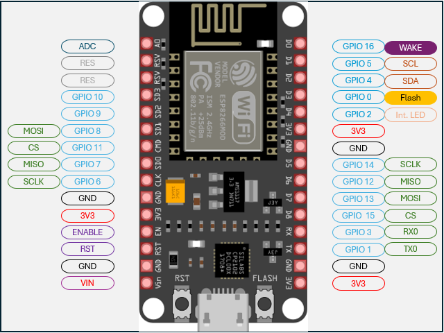
The pin assignment of the NodeMCU with 30 PINs is shown here. For the sake of clarity, this is a simplified representation. As a rule, many PINs are assigned more than once. I will go into this in more detail.

Here is a brief description of the function of the PINs.
| PIN Designation | Input | Output | Remark |
|---|---|---|---|
| A0 – ADC | Analog iIput | No Output | Measurement of analog values |
| D0 – GPIO 16 | No Interrupt | no PWM or I2C | High when booting! Low – WakeUp from DeepSleep |
| D1 – GPIO 5 | Digital Input | Digital Output | SCL for I2C at the same time |
| D2 – GPIO 4 | Digital Input | Digital Output | SDA for I2C at the same time |
| D3 – GPIO 0 | Pull UP | Digital Output | Is connected to flash button. LOW prevents booting |
| D4 – GPIO 2 | Pull Up | Digital Output | High when booting! Is connected to onboard LED. No booting at LOW |
| D5 – GPIO 14 | Digital Input | Digital Output | Serial Peripheral Interface SLCK (Serial Clock) – Clock line generated by the master |
| D6 – GPIO 12 | Digital Input | Digital Output | Serial Peripheral Interface MISO (Master In Slave Out) Data from slave to master |
| D7 – GPIO 13 | Digital Input | Digital Output | Serial Peripheral Interface MOSI (Master Out Slave In) Data from master to slave |
| D8 – GPIO 15 | Pull Down | Digital Output (restricted) | Serial Peripheral Interface CS (Chip Select) – Activation Slave – No booting at HIGH! |
| RX – GPIO 3 | Digital Input (restricted) | RX | HIGH when booting |
| TX – GPIO 1 | TX | Digital Input (restricted) | HIGH when booting. Debug faulty if LOW |
The most important functions of the individual PINs are shown above. The table also makes it clear what results we can expect from the assignment.
The I2c interface should be emphasized here. This is not a hardware interface, but is implemented via software.
A0 – Analog input
The ESP8266 12-E NodeMCU kit supports analog reading with PIN A0 or ADC0. Please note that this PIN has a maximum input voltage of 0-3.3 volts. Other ESP8266 boards only tolerate 0-1 volts. Please refer to the data sheet for your board.
Other PINs with multiple use
GPIO6 to GPIO11 are usually connected to the chip for flashing. These should not be used for other purposes.
GPIO0 is also labeled FLASH in the image above. This also corresponds to pressing the FLASH button.
GPIO0, GPIO1, GPIO2, GPIO3, GPIO9, GPIO10, GPIO15, GPIO16 assume certain levels during the boot process. Please refer to the table above under Remarks to find out which levels these are.
Please note that a connected relay, for example, can switch uncontrollably during the boot process if the level at the PIN becomes high or low.
The RST PIN is used to reset the board. The reset corresponds to pressing the RST button on the board.
A board that has been put into deep sleep can be woken up again via GPIO16 (WAKE). To do this, the PIN must be connected to the RST PIN.
In addition to the functions mentioned, the PINs GPIO0 to GPIO15 can be used for pulse width modulation (PWM). There will be a more detailed article on this.
This will give you a basic understanding of which PINs you can use safely and which PINs you should be careful with.
